
Belgium · Ghent
Ghent University
A leading European research university driven by innovation, critical thinking and a strong international outlook.
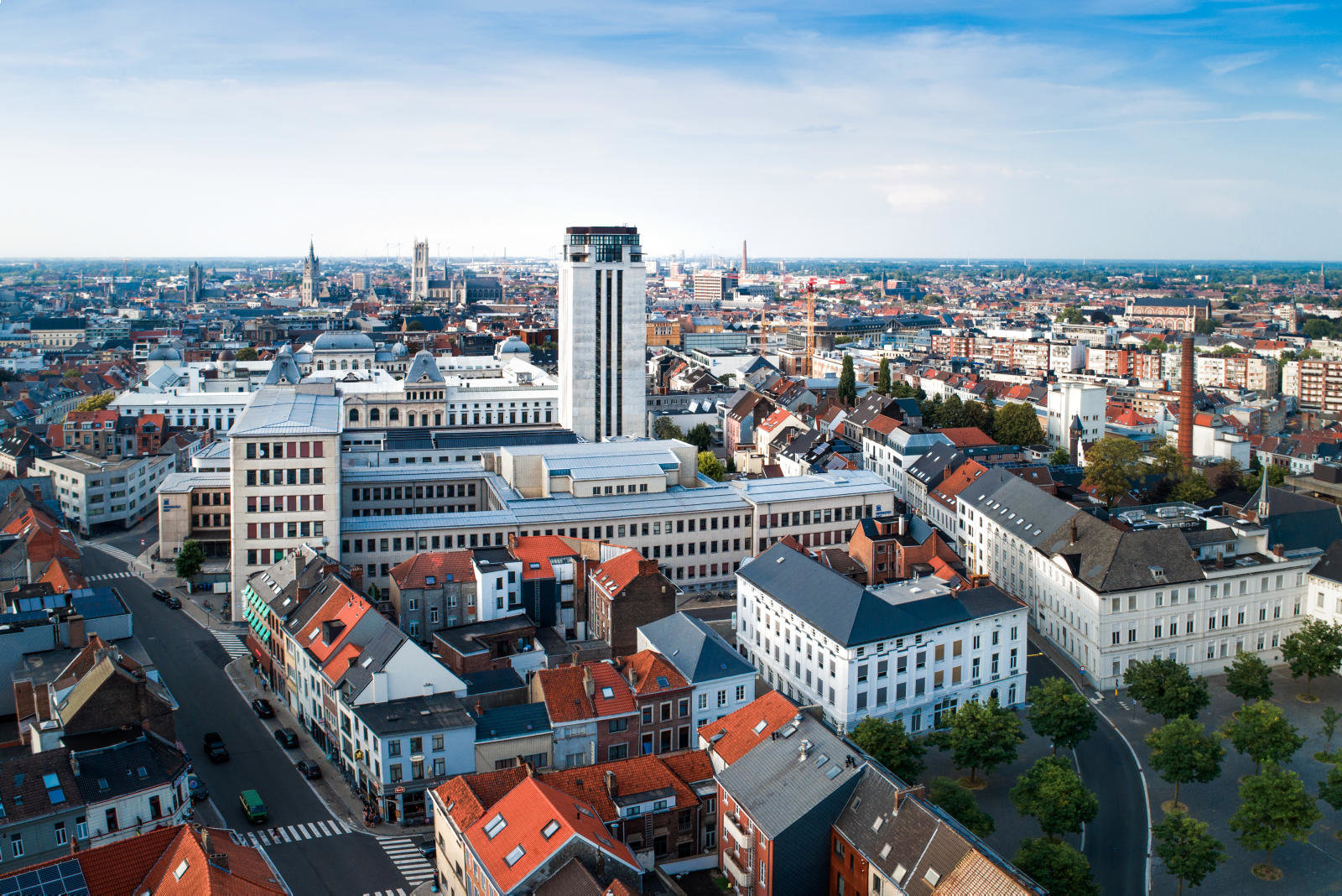
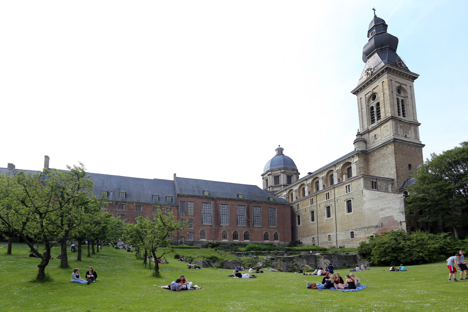
Ghent University is a top 100 university, founded in 1817, and one of the major universities in Belgium with 50,000 students and 15,500 employees. Our 11 faculties offer more than 200 programmes and conduct in-depth research within a wide range of scientific domains. Our credo is ‘Dare to Think’, challenging everyone to question conventional views and to dare to take a nuanced stand. We are a pluralistic university open to all, regardless of their ideological, political, cultural or social background. Ghent University Global Campus is also the first European university in Songdo, South Korea.


Faculty of Engineering and Architecture
The Faculty of Engineering and Architecture is one of the largest faculties of Ghent University. It combines state-of-the-art research with top-notch education in all significant engineering and architecture fields. The faculty strongly focusses on international relations. It offers a wide array of master’s programmes taught in English and is active in all major exchange programmes. Through research collaboration and educational links with top European institutions, the faculty strives to further enhance its international perspective.
Tech Lane Ghent Science Park – Campus Ardoyen
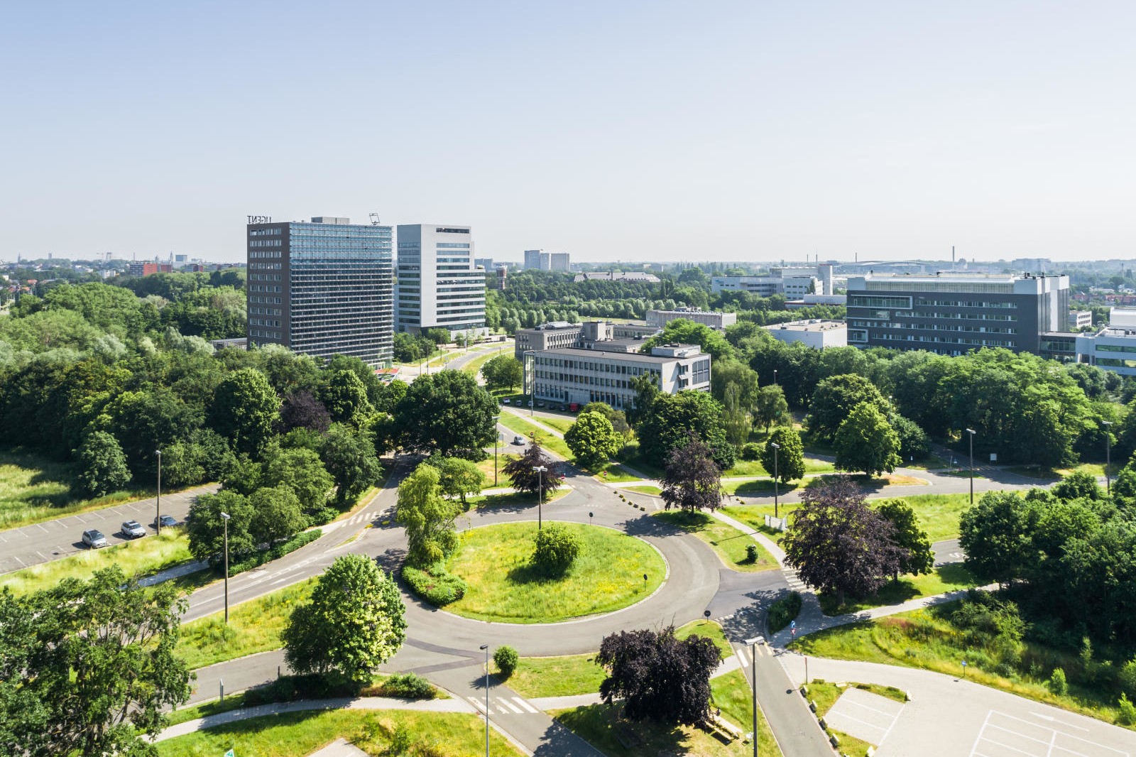
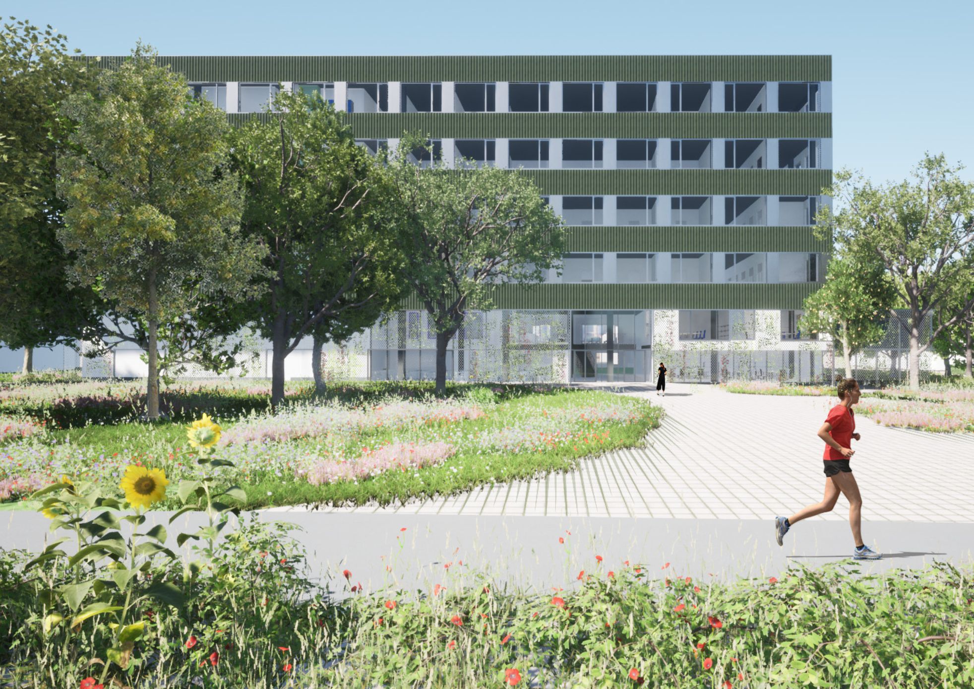
Tech Lane Ghent Science Park is a vibrant ecosystem of university labs and teaching facilities, international corporate R&D centers, and high-tech growth enterprises, providing a stimulating environment to promote innovation and entrepreneurship.
The Park currently hosts 11 university labs, 12 public research centres, 8 industrial pilots & testfacilities and more than 90 knowledge intensive start-ups, academic & corporate R&D centres, covering an integrated campus of 60 ha, housing more than 4,400 high-tech professionals. It also hosts the Ghent University Photonics ISO class 5 cleanroom for the fabrication of integrated integrated circuits (PICs) as well as the post processing of existing wafer scale PICs. It is equipped with mask aligners for UV photolithography, Voyager e-beam with sub 50 nm resolution, a Laser Direct Imaging transfert printer, polishing machine, wafer bonder, reactive ion etching, deposition tools via sputtering, PECVD, and spin coating, as well as inspection tools: ellipsometer, microscope, SEM, profilometer.


Disclaimer
Co-funded by the European Union. Views and opinions expressed are however those of the author(s) only and do not necessarily reflect those of the European Union or the European Education and Culture Executive Agency (EACEA). Neither the European Union nor EACEA can be held responsible for them.